
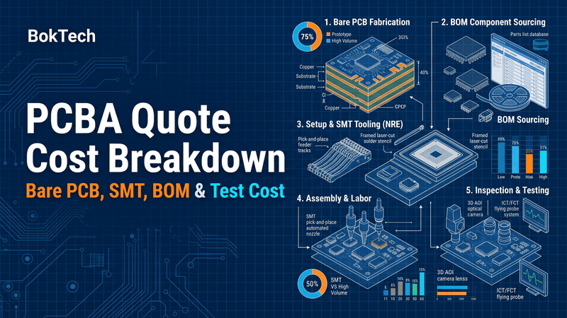
Quick Takeaway (TL;DR): A Printed Circuit Board Assembly (PCBA) quotation is not an arbitrary estimate for "a bare board with soldered parts." It is the weighted sum of five independent cost centers: bare-board fabrication (layer count, HDI microvias, laminate materials), BOM component procurement (typically 50% to 80% of total unit cost), one-time SMT setup and NRE tooling (stencils, pick-and-place feeder mapping, thermal reflow profiling), inspection and test coverage (3D SPI, 3D AOI, 3D AXI X-ray, ICT/FCT), and volume batch amortization. Submitting an ambiguous RFQ forces manufacturers to apply a 15% to 30% contingency risk buffer or triggers protracted engineering holds. Providing an audited data package with exact Manufacturer Part Numbers (MPNs), verified centroid rotation angles, and explicit IPC acceptance criteria guarantees a factory-accurate quote on the first pass.
1. The 5 Cost Pillars of a Turnkey PCBA Quotation
Understanding how cost centers shift across production volumes enables hardware engineering and procurement teams to design for cost optimization before committing to physical tooling:
| Cost Center Pillar | Primary Cost Drivers | Approximate Cost Share (Prototype: 10 pcs) | Approximate Cost Share (Production: 10k pcs) | Primary Engineering Levers for Cost Reduction |
| 1. Bare-Board Substrate | Layer count, HDI microvias, base laminates (FR-4 vs Megtron), copper weight | 15% to 25% | 10% to 20% | Optimize panel utilization (> 85%); standardize layer stack-ups |
| 2. BOM Component Sourcing | Active silicon, discrete passives, supply-chain allocations, packaging | 35% to 50% | 65% to 80% | Designate verified second-source alternates; consolidate unique line items |
| 3. Setup & Tooling NRE | Laser-cut stencils, SMT feeder setup, First-Article Inspection (FAI) | 25% to 40% | < 2% (Fully amortized) | Reduce unique part numbers (feeder setups); standardize package sizes |
| 4. Assembly & Labor | Double-sided SMT passes, selective wave soldering, manual through-hole | 10% to 15% | 5% to 10% | Eliminate manual hand soldering; convert all THT to surface-mount |
| 5. Inspection & Testing | 3D SPI, 3D AOI, 3D AXI radiographic inspection, custom ICT/FCT | 5% to 10% | 3% to 8% | Standardize test-point grids; automate functional test sequences |
2. Bare-Board Fabrication Drivers: Setting the Substrate Cost Floor
The bare circuit board establishes the physical and electrical cost baseline of the assembly quotation before any component reel is loaded onto an SMT feeder:
•Layer Count and HDI Build-Up: Each additional layer pair increases sequential lamination, mechanical drilling, and chemical plating cycles. A standard 8-layer through-hole board costs significantly less than an 8-layer 1+N+1 or 2+N+2 HDI board requiring laser microvias and Via-in-Pad Plated Over (VIPPO).
•Laminate Material Selection: Standard FR-4 (Tg 140°C–150°C) is the industry cost baseline. Stepping up to high-Tg laminates (Tg ≥ 170°C), halogen-free substrates, or ultra-low-loss materials (such as Panasonic Megtron 6/7 or Rogers 4000 series for RF/high-speed compute) increases bare laminate costs by 80% to 200%.
•Panel Utilization Efficiency: PCB manufacturers process standardized production panels (e.g., 18" × 24" or 21" × 24"). An irregular board outline or inefficient panelization array that achieves only 60% panel utilization wastes 40% of the raw copper-clad laminate, directly inflating unit costs.
•Surface Finish and Special Processes: Lead-Free Hot Air Solder Leveling (HASL) represents the lowest cost finish but is incompatible with fine-pitch BGAs. Electroless Nickel Immersion Gold (ENIG) adds 5% to 15% to bare-board costs but ensures pad planarity. Advanced finishes like ENEPIG, hard gold fingers, castellated edges, and controlled-depth back-drilling introduce specialized chemical and CNC routing passes.
| Bare PCB Parameter | Baseline Specification (Lowest Cost) | Premium Specification (Moderate Cost) | High-Complexity Driver (Highest Cost) |
| Layer Architecture | 2 to 6 Layers; Standard Through-Hole | 8 to 14 Layers; Blind/Buried Vias | 16 to 32+ Layers; Any-Layer HDI (VIPPO) |
| Dielectric Material | Standard FR-4 (Tg 130°C–140°C) | High-Tg FR-4 (IT-180A, S1000-2M) | Panasonic Megtron 6/7; Rogers RF hybrid |
| Finished Copper Weight | 1.0 oz (35 µm) outer / inner | 2.0 oz (70 µm) inner power planes | 3.0 oz to 5.0 oz (Heavy copper PDN) |
| Surface Finish | Lead-Free HASL | ENIG (2–3 µin Gold / 120–200 µin Nickel) | ENEPIG; Hard Gold (30 µin Gold for contacts) |
| Trace / Space Minimum | ≥ 5 mil / 5 mil (0.127mm) | 4 mil / 4 mil (0.100mm) | ≤ 3 mil / 3 mil (0.075mm, fine-line yield risk) |
Review our PCB manufacturing services for detailed fabrication capabilities, consult our PCB fabrication specification guide for data requirements, and explore layer stackup tolerances and impedance to evaluate standard stack-up guidelines.
3. Component Procurement & BOM Dynamics: Managing the 50% to 80% Variable
On high-density computing and mixed-signal assemblies, electronic components represent the largest line item on the quote. The Bill of Materials (BOM) is also the primary origin of quoting delays and pricing revisions.
Unique Part Count vs. Total Placements
SMT line setup time is governed by the number of unique line items (distinct component reels, tubes, and matrix trays), not merely total placement count. Loading 1,000 instances of a single 0402 decoupling capacitor requires one feeder setup; loading 1,000 components distributed across 120 unique part numbers requires extensive feeder bank configuration, optical feeder calibration, and component verification.
Package Complexity and Process Routing
The package mix dictates the required assembly technologies:
•Ultra-Fine Pitch Components: 0.35mm–0.50mm micro-BGAs, Wafer-Level Chip-Scale Packages (WLCSP), and 01005 passives require high-accuracy placement heads, laser-cut step stencils, Type 4 or Type 5 solder paste, and automated 3D X-ray inspection.
•Mixed Technology (SMT + Through-Hole): Boards requiring through-hole technology (THT) connectors, power transformers, or large electrolytic capacitors introduce selective wave soldering or manual hand soldering passes, significantly increasing touch labor costs.
Sourcing Models: Turnkey vs. Consigned vs. Hybrid
•Full Turnkey: The PCBA manufacturer procures 100% of the components through authorized global distributors (Mouser, Digi-Key, Element14, Arrow) and direct factory channels. The manufacturer manages lead times, minimum order quantity (MOQ) overages, and counterfeit risks.
•Consigned (Kitted): The customer purchases and delivers all parts to the assembly plant. While component procurement markups are eliminated, the customer absorbs shipping freight, customs clearance delays, and component attrition buffers.
•Hybrid: The customer supplies proprietary or long-lead ICs (such as pre-programmed microcontrollers or custom ASICs), while the manufacturer procures standard passives, connectors, and discrete semiconductors.
| BOM Flaw / Inaccuracy | Quoting & Procurement Impact | Manufacturing Consequence | Engineering Resolution |
| Missing Exact MPN (e.g., "10k resistor 0402") | Quoting stalled; automated ERP API pricing fails | Incorrect tolerance, voltage rating, or temp coefficient placed | Provide full manufacturer part numbers (e.g., RC0402FR-0710KL) |
| No Approved Alternates | Delays if primary MPN is allocated or has an 18-week lead time | Line stoppage or expensive spot-market broker markups | Designate 2 to 3 pin-compatible second-source alternates in BOM |
| Loose / Cut-Tape Packaging | SMT feeders cannot load short cut tapes under 12 inches without leaders | Manual component feeding or re-reeling fees; higher component attrition | Order components in continuous tape on reels with leaders and trailers |
| Unstated Moisture Sensitivity | Failure to allocate pre-bake cycle times (MSL 3, 4, 5a) | Component package delamination ("popcorning") during reflow | Flag MSL levels in BOM notes so baking schedules are priced into setup |
For full file preparation guidelines, see our comprehensive PCB manufacturing files guide.
4. One-Time Setup Costs (NRE) and SMT Line Preparation
Non-Recurring Engineering (NRE) and setup costs are fixed expenses incurred once per production run. These fixed costs explain why a prototype batch of 5 boards carries a dramatically higher per-unit price than a production run of 1,000 boards:
Amortized Setup Cost Formula: Setup Cost Per Board = Total Setup NRE Fees ÷ Production Batch Quantity
•Solder Paste Stencils: High-density SMT layouts require electro-polished laser-cut stainless steel stencils (typically 100 µm to 130 µm foil thickness). Boards pairing 0.4mm micro-BGAs with high-current power inductors often require specialized multi-level step-down stencils to deposit distinct paste volumes across different pad geometries.
•SMT Pick-and-Place Programming: Automated lines require translation of the layout centroid (XY coordinate / Pick-and-Place / CPL) file into machine placement programs. Clean centroid files with clear component rotation conventions (IPC-7351 standard) eliminate manual part alignment delays.
•Thermal Profiling (Reflow & Wave): Profiling engineers instrument a physical sample board with multiple thermocouple sensors to map the preheat slope, soak time, time above liquidus (TAL), and peak reflow temperatures across light and heavy thermal masses.
•First-Article Inspection (FAI): Before releasing the line for batch assembly, a dedicated technician inspects the first assembled board using optical and electrical tools to verify every component value, orientation, and polarity against the golden BOM.
| Order Batch Size | Laser Stencil Cost ($) | SMT Line Setup & Programming ($) | First-Article Inspection ($) | Total Setup NRE ($) | Setup Cost Amortized Per Board ($) |
| 5 Boards (Rapid Prototype) | $120 | $200 | $150 | $470 | $94.00 per board |
| 50 Boards (Pilot Run) | $120 | $200 | $150 | $470 | $9.40 per board |
| 500 Boards (Low-Volume) | $150 (Framed) | $250 | $150 | $550 | $1.10 per board |
| 5,000 Boards (Mass Production) | $200 (Multi-up) | $350 | $200 | $750 | $0.15 per board |
Consult our guide on PCBA specification: assembly tolerances and acceptance criteria to evaluate quality metrics that apply to first-article approvals.
5. Inspection, Quality Verification, and Electrical Testing Costs
Testing and quality assurance parameters are frequently overlooked during quote comparisons, leading to misleading apples-to-oranges evaluations between suppliers offering vastly different test scopes.
Automated Inspection Layers
•3D Solder Paste Inspection (SPI): Measures the height, area, volume, and registration of printed solder paste before components are placed, catching over 70% of potential SMT soldering defects.
•Pre-Reflow & Post-Reflow Automated Optical Inspection (AOI): Post-reflow 3D AOI uses multi-angle cameras and laser triangulation to verify component presence, value markings, polarity, skew, tombstoning, and solder fillet formation.
•3D Automated X-Ray Inspection (AXI): Essential for area-array packages (BGA, WLCSP, LGA) and bottom-terminated components (QFN, DFN) where solder joints are hidden beneath the package. AXI validates solder ball wetting, detects bridging, and quantifies thermal pad voiding percentages.
Electrical and Functional Testing
•In-Circuit Testing (ICT) / Flying Probe: Flying probe testing uses automated moving needles to test individual net continuity, resistance, capacitance, and basic diode operation without custom tooling fixtures. Bed-of-nails ICT fixtures test the entire board simultaneously in seconds, making them standard for volume runs despite higher initial fixture tooling costs ($1,500–$4,000).
•Functional Testing (FCT): Validates actual operational behavior under power. FCT ranges from simple "power-on and LED blink" checks to full bus loopback, RF sensitivity, and firmware flashing protocols. Quoting FCT requires clear procedural documentation, cycle time estimates, and defined failure handling routines.
| Quality Verification Tier | Inspection Methods Deployed | Typical Defect Coverage | Testing Cycle Time per Board | Relative Cost Impact |
| Tier 1: Standard Visual | Manual visual inspection + Lead-Free AOI | Gross solder bridging, missing parts | 15 to 30 seconds | Baseline (Included in standard SMT) |
| Tier 2: High-Density Industrial | 100% 3D SPI + 3D AOI + Sample 3D X-ray | Solder volume, joint fillets, BGA alignment | 45 to 90 seconds | +5% to +10% over standard SMT |
| Tier 3: Mission-Critical Compute | 100% 3D SPI + 100% 3D AXI + Flying Probe | BGA voiding (< 15%), net shorts, component values | 3 to 10 minutes | +15% to +30% assembly cost |
| Tier 4: Complete Turnkey FCT | Tier 3 + Custom Bed-of-Nails ICT + Functional Test | Full hardware logic, firmware, and bus verification | 1 to 5 minutes | Requires custom fixture NRE ($1.5k–$5k) |
Explore our equipment and inspection capabilities to review the verification systems active on our production floors.
6. Pre-Quote Engineering Checklist: Eliminating the "Vague Request" Penalty
When an RFQ package contains missing files or ambiguous specifications, quoting engineers cannot compute precise manufacturing cycle times. To protect against yield loss and scope creep, quotation systems apply conservative assumptions and contingency pricing buffers (typically inflating initial estimates by 15% to 30%).
Providing a structured, verified data package guarantees an accurate quote on the initial submission:
| Engineering Input Group | Non-Negotiable Documentation Required | Why It Matters for Quoting Accuracy | Financial Risk If Omitted |
| 1. Fabrication Artwork | RS-274X Gerber or ODB++, drill files, board outline | Determines layer count, hole density, routing complexity | Quote stalls pending layer/outline clarification |
| 2. BOM Dataset | Excel/CSV with Manufacturer, exact MPN, Description, Package, Designator, Qty | Allows automated ERP distributor API pricing and lead time checks | Generic descriptions produce padded component estimates |
| 3. Approved Alternates | 1 to 2 acceptable alternate MPNs for high-risk/allocated parts | Enables supply-chain purchasing flexibility if lead times spike | Schedule delays or secondary spot-market broker fees |
| 4. Component Placement | Centroid (XYRS / Pick-and-Place) file with clear 0° rotation convention | Sets SMT placement machine run times and feeder allocations | Feeder programming delays; orientation mismatches |
| 5. Assembly Drawings | PDF showing mechanical hardware, pin-1 markers, polarity indicators | Resolves package ambiguity (e.g., diodes, polarized capacitors) | Component polarity reversals during first-article setup |
| 6. Testing Specification | Written test plan, required fixtures, firmware programming requirements | Establishes technician cycle time and fixture tooling investments | Testing omitted from quote or priced on rough hourly estimates |
| 7. Order Scope | Exact quantities, delivery schedule, consigned vs. turnkey split | Dictates component volume pricing tiers and machine scheduling | Inability to calculate bulk distributor discounts |
Consult our frequently asked questions for common BOM formatting inquiries, and read our comprehensive startup hardware manufacturing guide for end-to-end guidance from prototype to volume delivery.
7. Frequently Asked Questions (FAQ)
Why is a 5-board prototype PCBA quote so much more expensive per unit than a 500-board run?
In a 5-piece prototype run, fixed Non-Recurring Engineering (NRE) costs—including laser-cut SMT stencils ($100–$200), pick-and-place feeder setup ($150–$300), and First-Article Inspection ($100–$200)—are divided across only 5 units, adding $70 to $140 in overhead to each board. Additionally, component distributors charge single-unit pricing rather than full-reel volume discount rates.
What causes the longest delays during the PCBA quoting process?
Incomplete or ambiguous BOM data causes over 80% of quotation delays. Common issues include listing distributor part numbers instead of original manufacturer part numbers (MPNs), leaving component package footprints blank, omitting designator counts, or failing to identify which lines are customer-consigned versus turnkey-sourced.
Can I reduce my PCBA quote by supplying my own parts (consigned build)?
Consignment can reduce cash outlay if you already hold inventory of expensive, specialized ICs. However, for standard passives, discrete transistors, and common connectors, turnkey procurement through an established manufacturer is typically cheaper due to high-volume distributor discounts. Consigned builds also risk project delays if parts are delivered in cut tape without proper leaders, requiring costly manual re-reeling.
How does choosing ENIG over Lead-Free HASL affect the overall assembly quote?
ENIG increases the bare-board fabrication price by approximately 5% to 15% compared to Lead-Free HASL. However, for boards utilizing fine-pitch BGAs (≤ 0.8mm), QFNs, or 0402/0201 passives, ENIG provides an ultra-flat, planar surface that prevents component skew and bridging. This higher bare-board cost is offset by significantly higher SMT assembly yields and reduced rework expenses.
8. From Prototype to Volume PCBA Production: Partner with BokTech
Navigating the transition from an initial prototype run to high-yield, cost-optimized volume PCBA production introduces severe technical and supply chain hurdles:
•Mitigating solder bridging and voiding across 0.35mm–0.50mm micro-BGAs and high-density QFN thermal pads.
•Managing component obsolescence, long lead times, and single-source silicon allocations without compromising schedules.
•Developing robust, high-coverage functional test fixtures that catch edge-case hardware faults before final box build.
•Maintaining rigid IPC-A-610 Class 2 and Class 3 assembly standards across expanding production batches.
BokTech delivers end-to-end turnkey PCB manufacturing, strategic global component sourcing, and high-precision SMT assembly from our advanced manufacturing center in Shenzhen. We provide:
•Complete Bare-Board Fabrication: 1 to 32 layer multi-layer, Any-Layer HDI, heavy copper (up to 5 oz), and specialized high-frequency hybrid laminates (Megtron 6/7, Rogers, high-Tg FR-4).
•Turnkey Component Procurement: Direct partnerships with authorized global component distributors, integrated in-house component authentication, and automated counterfeit inspection.
•High-Precision SMT & THT Lines: Fully automated placement lines capable of 01005 passives, 0.35mm micro-BGAs, Package-on-Package (PoP), and nitrogen-purged reflow soldering.
•Advanced Quality Verification: 100% 3D Solder Paste Inspection (SPI), multi-angle 3D AOI, high-resolution 3D Automated X-Ray (AXI), flying probe testing, and custom functional testing (FCT).
•Free Engineering DFM & BOM Analysis: Every order undergoes thorough pre-production Design for Manufacturability (DFM) and Design for Assembly (DFA) audits, catching BOM inconsistencies and footprint errors before production lines are scheduled.
For deeper technical guidance on bare-board parameters, explore our PCB fabrication specification guide, review our PCB manufacturing files guide, and consult our guide on PCB assembly services: prototype to low-volume.
Ready to optimize your production costs and receive a transparent, factory-direct quotation? Upload your PCB files and BOM for an instant quotation, or contact our engineering team for a comprehensive DFM and BOM review.


{{ commentCount }} Comments