
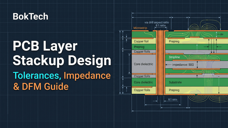
Quick Takeaway (TL;DR): The PCB layer stack-up is the foundational manufacturing decision that physically hardens your design. While schematic connections and component placement can be revised, a laminated stack-up permanently establishes transmission line impedance, dielectric loss, mechanical stiffness, thermal dissipation, and drill aspect ratios. Standard finished board thickness follows a ±10% fabrication tolerance (tightened to ±8% or ±0.10mm for PCIe edge-card contacts). To prevent costly scrap, stack-up design must enforce three engineering baselines: maintaining mechanical drill aspect ratios ≤ 10:1, compensating trace spacing by 1.0 to 2.0 mils per additional ounce of copper weight, and mirroring dielectric and copper mass within ±10% across the center line to eliminate dynamic reflow warpage (bow and twist).
1. Why the Stack-Up Dictates the Entire Fabrication Workflow
A PCB layer stack-up is not a passive bill of materials; it is an active multi-physics structure that couples electrical wave propagation, fluid lamination dynamics, and thermal expansion.
When Computer-Aided Manufacturing (CAM) engineers open a data package, the stack-up defines every downstream manufacturing constraint:
| Stack-Up Parameter | Immediate Manufacturing Dependency | Downstream Electrical & Physical Consequence | Primary Scrap Risk If Flawed |
| Layer Ordering & Function | Reference plane assignment & return paths | High-speed return current loops, loop inductance, and EMI | Severe crosstalk and inter-symbol interference (ISI) |
| Dielectric Thickness (H) | Prepreg glass style selection & resin content | Characteristic trace impedance (Z0) and inter-plane capacitance | Impedance drift outside ±10%; high-speed eye closure |
| Finished Copper Weight | Chemical etching dwell time & etch factor compensation | DC current carrying capacity, IR drop, and minimum feature spacing | Trace neck-down, open circuits, or pad delamination |
| Core & Prepreg Symmetry | Vacuum thermal lamination press cycles | Coefficient of Thermal Expansion (CTE) balance across Z/X/Y axes | Reflow bow and twist (> 0.75%), causing fractured BGA joints |
| Total Laminated Thickness | Mechanical CNC drill depth & plating cycle times | Plating aspect ratio and chemical exchange through via barrels | Center-barrel plating starvation and early via fatigue failure |
2. Layer Count Architecture: Signal, Power, and Plane Interleaving
Layer count is an outcome of required routing channels, power rail isolation, and continuous reference plane assignments. Two boards sharing an identical 8-layer count will deliver entirely different signal integrity depending on how layers are allocated.
Plane Assignment and Return-Path Grounding
•Microstrip Layers (Outer): Traces routed on external layers reference a single adjacent internal solid ground plane. Outer traces exhibit higher propagation velocity but radiate more electromagnetic energy.
•Stripline Layers (Inner): High-speed differential pairs sandwiched between two continuous ground reference planes benefit from complete electrostatic shielding and uniform dielectric properties.
•Interleaved Power and Ground: Placing power planes within 2 to 3 mils of solid ground planes maximizes planar capacitance, suppressing high-frequency transient noise above 200 MHz before discrete decoupling capacitors can respond.
| Board Layer Count | Standard Layer Sequence Allocation | Reference Plane Coupling Strategy | Primary Engineering Application | Warpage Sensitivity |
| 4-Layer Multilayer | L1: Sig, L2: GND, L3: PWR, L4: Sig | Outer signals reference adjacent solid planes | Microcontrollers, standard IoT, low-speed sensors | Low (Symmetric 1-core build) |
| 6-Layer Multilayer | L1: Sig, L2: GND, L3: Sig, L4: PWR, L5: GND, L6: Sig | Inner stripline on L3 referenced to GND and PWR | Embedded Linux SoCs, DDR3/DDR4, PCIe Gen 3 | Moderate (Requires balanced prepreg) |
| 8-Layer High-Speed | L1: Sig, L2: GND, L3: Sig, L4: GND, L5: PWR, L6: Sig, L7: GND, L8: Sig | Dual stripline routing channels with isolated ground shields | Multi-gigabit Ethernet, PCIe Gen 4, LPDDR4X | Moderate to High |
| 12 to 16 Layer Multi-Rail | Alternating Signal-Ground-Signal-Ground-Power topology | Complete stripline isolation; dedicated 2 oz core PDN | AI edge accelerators, multi-FPGA systems | High (Requires exact copper balance) |
For advanced microvia escape routing and sequential lamination rules, review our HDI and microvia builds capabilities.
3. Finished Thickness, Dielectric Tolerances, and Drill Aspect Ratio
Finished thickness is the cumulative sum of raw copper foils, cured prepreg plies, dielectric cores, surface plating, and soldermask layers.
Finished Board Thickness Tolerances
•Standard Manufacturing Tolerance: ±10% of nominal thickness (e.g., a standard 1.60mm board ranges from 1.44mm to 1.76mm).
•Tight Mechanical Tolerance: ±8% or ±0.10mm, strictly required for edge-card contacts (such as PCIe add-in cards or DIMM modules) to ensure gold fingers seat securely inside socket card guides.
•Soldermask & Plating Thickness Contribution: Outer electroplated copper adds approximately 25 µm to 35 µm per side, while liquid photoimageable (LPI) soldermask adds 15 µm to 25 µm over bare laminate.
Drill Aspect Ratio Limits
The drill aspect ratio represents the mechanical and chemical plating boundary of the fabrication plant:
Drill Aspect Ratio Formula: Aspect Ratio = Finished Board Thickness (mm) ÷ Smallest Drilled Tool Diameter (mm)
•Standard Through-Hole Baseline: Aspect ratios up to 8:1 to 10:1 can be reliably plated using standard vertical electroplating lines.
•Advanced High-Aspect Ratio: Ratios between 10:1 and 12:1 require continuous fluid movement and periodic pulse reverse electroplating to force copper ions into the center of the via barrel.
•Physical Defect Risk: If an aspect ratio exceeds 10:1 without dedicated plating adjustments, the center of the through-hole barrel suffers from thin copper plating (< 15 µm), resulting in via fatigue fractures during lead-free reflow (240°C–260°C).
| Mechanical & Stack-Up Feature | Standard Commercial Tolerance | High-Reliability / IPC Class 3 Tolerance | Physical Scrap Risk If Uncontrolled |
| Overall Board Thickness | ± 10% of nominal | ± 8% (or ± 0.10mm for edge connectors) | Connector insertion failure or loose electrical contact |
| Mechanical Drill Diameter | ± 0.08mm (± 0.003 in) | ± 0.05mm (± 0.002 in) | Component pin interference or poor solder wicking |
| Mechanical Aspect Ratio | ≤ 8:1 (Standard processing) | Up to 10:1 or 12:1 (Advanced pulse plating) | Center via barrel cracking under thermal expansion |
| Laser Microvia Aspect Ratio | ≤ 0.8:1 (Standard laser drill) | ≤ 1.0:1 (Targeted solid copper fill) | Microvia barrel separation from target landing pad |
| Dielectric Layer Thickness | ± 10% (Prepreg nominal) | ± 7% (Laser measurement controlled) | Severe impedance drift on RF and high-speed SERDES |
4. Copper Weight and Etch Compensation Rules
Copper weight directly governs trace geometry. Chemical etching sprays acidic or alkaline chemistry to dissolve unwanted copper foil; thicker copper foils take longer to dissolve, creating a trapezoidal trace cross-section known as the etch factor (undercut).
Ready to manufacture your multi-layer PCB or custom PCBA? Upload your PCB files for an instant quotation, or contact our engineering team today for a complete DFM and stack-up review.


{{ commentCount }} Comments