
PCB Design
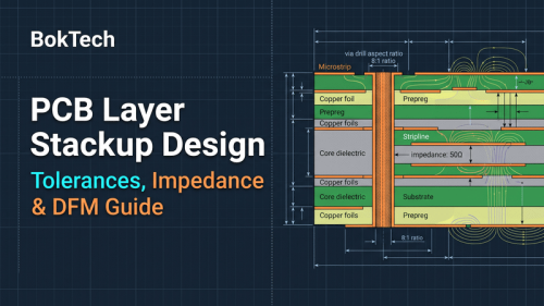
PCB Layer Stackup Design: Tolerances, Impedance & DFM Guide
Master PCB layer stackup design: finished thickness tolerances, copper etch compensation, drill aspect ratios, and controlled impedance fabrication notes.