
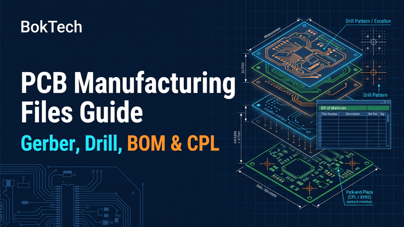
Quick Takeaway (TL;DR): A production-ready PCB release package is never a single Gerber file; it is an integrated, cross-referenced data package. Bare-board fabrication requires RS-274X or ODB++ artwork, Excellon drill files sharing an identical origin (0,0), and a Master Fabrication Drawing defining layer stack-up, dielectric materials, copper weights, and IPC-6012 Class 2/3 tolerances. Turnkey assembly (PCBA) mandates three additional deliverables: an exact Bill of Materials (BOM) with verified Manufacturer Part Numbers (MPNs) and approved alternates, an XYRS Centroid (Pick-and-Place / CPL) file with defined 0° rotation conventions, and an Assembly Drawing showing pin-1 and polarity indicators. Over 75% of pre-production DFM holds stem from data package discrepancies—such as drill-to-copper coordinate offsets, unstated component rotation conventions, or revision mismatches between BOM and Gerber files.
1. The Dual-Domain Data Package: Bare-Board vs. Assembly Requirements
A common mistake during engineering handoff is submitting a disorganized archive where bare-board fabrication parameters are buried inside assembly notes, or critical component data is missing entirely.
A production release must clearly separate bare-board fabrication data from component assembly data:
| Manufacturing Domain | Primary Deliverables | Target Engineering Audience | Essential Cross-Check Requirement |
| Bare-Board Fabrication | Gerber RS-274X or ODB++, Excellon Drill files, IPC-D-356 Netlist, Master Fab Drawing | PCB CAM engineers, lamination & wet chemistry technicians | Drill origin matches copper artwork; layer stackup matches drawing |
| SMT & THT Assembly (PCBA) | Structured BOM (Excel/CSV), Centroid (Pick-and-Place) file, Assembly Drawing (PDF), Paste Gerber | SMT programming engineers, quality inspectors, test technicians | BOM reference designators match Centroid coordinates and CAD silk |
| Testing & Verification | Electrical test fixture files, Flying probe netlist, Functional Test (FCT) procedures | Quality assurance & test fixture engineers | Test points clear of component bodies; firmware flashing guides provided |
2. Artwork Standards: RS-274X Gerber vs. ODB++
Artwork files represent the two-dimensional vector geometry of every physical layer in the printed circuit board.
Gerber RS-274X / Gerber X2
RS-274X remains the industry standard, embedding aperture definitions, polygon fills, and coordinate data within each individual layer file. Gerber X2 builds upon this by adding metadata (such as layer function, via types, and copper profile attributes).
To prevent CAM engineers from guessing layer order, apply unambiguous file naming that explicitly includes the layer number and functional name:
| Layer Function | Recommended File Naming Convention | Altium Designer Default | KiCad Default | Cadence Allegro Default |
| Top Copper (L1) | L01_Top_Copper.gbr | Project.GTL | Project-F_Cu.gbr | top.art |
| Inner Ground Plane (L2) | L02_GND01_Plane.gbr | Project.GP1 | Project-In1_Cu.gbr | gnd.art |
| Inner Signal Layer (L3) | L03_Signal01.gbr | Project.G1 | Project-In2_Cu.gbr | sig1.art |
| Bottom Copper (L4) | L04_Bottom_Copper.gbr | Project.GBL | Project-B_Cu.gbr | bottom.art |
| Top Solder Mask | L00_Top_SolderMask.gbr | Project.GTS | Project-F_Mask.gbr | soldtop.art |
| Bottom Solder Mask | L99_Bottom_SolderMask.gbr | Project.GBS | Project-B_Mask.gbr | soldbot.art |
| Top Silkscreen (Legend) | L00_Top_Silkscreen.gbr | Project.GTO | Project-F_Silks.gbr | silktop.art |
| Top Solder Paste (SMT) | L00_Top_Paste.gbr | Project.GTP | Project-F_Paste.gbr | pastetop.art |
| Board Outline / Profile | L00_Board_Outline.gbr | Project.GKO / GM1 | Project-Edge_Cuts.gbr | outline.art |
Mechanical Layer Rule: Always output the finished board outline on its own dedicated mechanical layer. Do not embed the board outline inside copper, soldermask, or silkscreen files, as this can trigger unintended copper clearance cutouts in CAM tooling.
ODB++: The Intelligent Manufacturing Alternative
ODB++ replaces dozens of individual Gerber and drill files with a single structured directory hierarchy carrying layer sequences, stack-up thicknesses, drill definitions, component footprints, and netlist data. Utilizing ODB++ drastically reduces pre-production DFM interpretation errors. If delivering ODB++, always include a PDF copy of your Master Fabrication Drawing so that stack-up assumptions and material callouts can be independently validated.
For a deeper look at artwork data, consult our PCB design services overview and our comprehensive guide on RS-274X Gerber file specifications.
3. Drill Data and Hole Definitions
Drill data directs the automated CNC mechanical drilling and laser drilling machinery. Missing or misaligned drill data is a primary source of immediate DFM holds.
Coordinate Origin and Unit Alignment
Drill files (Excellon format) must share the exact same coordinate origin (0,0), unit system (metric/inch), and resolution format as the copper artwork files. When drill files use absolute coordinates while Gerber files use relative coordinates, the drill layer will appear shifted or scaled improperly when imported into CAM software.
Finished Hole Size (FHS) vs. Tool Size
Fabrication drawings must specify whether the dimensions in the drill chart represent Finished Hole Sizes (FHS) or Tool Diameters (Drill Bit Sizes):
•Finished Hole Size (Standard): The internal diameter of the hole barrel after chemical desmear and electroplating (which deposits 20 µm to 35 µm of copper). The fabricator applies automatic drill compensation (+0.10mm to +0.15mm) to select the correct starting tool bit.
•Plated vs. Non-Plated Holes: Clearly separate Plated Through-Holes (PTH) from Non-Plated Through-Holes (NPTH). Generating separate drill files (e.g.,
Drill_PTH.drlandDrill_NPTH.drl) ensures non-plated mounting holes are not routed through electroplating baths.
| Hole Classification | Standard Finished Hole Tolerance | Inspection Criteria | Manufacturing Notes Required |
| Standard Via Hole | + 0.08mm / - 0.08mm (± 3 mil) | IPC-6012 Class 2 / Class 3 | Specify tenting, epoxy plugging, or VIPPO capping |
| Component Lead Hole | + 0.08mm / - 0.05mm (+ 3 / - 2 mil) | Solder fill around lead pin | Requires PTH designation; minimum 10 mil annular ring |
| Press-Fit Connector Hole | + 0.05mm / - 0.025mm (+ 2 / - 1 mil) | Strict compliant pin retention | Must be explicitly flagged in drill notes for special tool calibration |
| Tooling / Mounting NPTH | + 0.05mm / - 0.05mm (± 2 mil) | Mechanical standoff retention | Must be non-plated with minimum 8 mil copper pull-back |
| Laser Microvia (HDI) | + 0.025mm / - 0.025mm (± 1 mil) | Solid copper plating fill | Specify layer transition pairs (e.g., L1-L2, L2-L3) |
If your design utilizes blind/buried vias or laser microvias, consult our HDI and microvia builds capabilities.
4. The Production-Grade BOM: Sourcing and SMT Efficiency
The Bill of Materials (BOM) drives component procurement, feeder loading, and surface-mount assembly. A flawed BOM stalls both automated quoting engines and manual purchasing reviews.
Non-Negotiable BOM Data Fields
Structure your BOM in standard spreadsheet formats (CSV, XLS, XLSX) using the following column organization:
| Column Field Header | Example Data Entry | Engineering Purpose | Quoting & Assembly Impact If Omitted |
| 1. Item Number | 1, 2, 3 | Line-item index | Sourcing and tracking ambiguity |
| 2. Reference Designators | C101, C102, C103 | Maps parts to board locations | SMT placement machines cannot assign components |
| 3. Quantity per Board | 3 | Total component count | Procurement quantity calculations fail |
| 4. Manufacturer | Murata Electronics | Locks component origin | Prevents unauthorized component substitution |
| 5. Exact MPN | GRM155R71C104KA88D | Uniquely identifies part parameters | Generic descriptions (e.g., "0.1uF cap") halt quoting |
| 6. Package / Footprint | 0402 (1005 Metric) | Verifies SMT pad land pattern | Footprint mismatches caught only during first-article setup |
| 7. Description | CAP CER 0.1UF 16V X7R 0402 | Functional engineering overview | Secondary verification of component characteristics |
| 8. Approved Alternates | Yageo: CC0402KRX7R7BB104 | Authorizes immediate second-sourcing | Eliminates production line stoppages if primary MPN is allocated |
| 9. Sourcing Type | Turnkey or Consigned | Defines procurement responsibility | Billing errors and delayed component handoffs |
Managing Do-Not-Fit (DNF / DNP) Parts
Do-Not-Fit parts must be explicitly designated in the BOM itself (e.g., entering "DNF" or "DNP" in a dedicated Fit Status column). Do not simply delete unplaced parts from the BOM while leaving them on the silkscreen artwork, as this triggers discrepancy flags during DFM audits.
Review our frequently asked questions for common BOM formatting inquiries.
5. Centroid (Pick-and-Place / CPL) and Assembly Drawings
The Centroid file (Component Placement List / CPL / XY data) provides machine-readable coordinate instructions for automated SMT pick-and-place systems.
Centroid File Format Requirements
The centroid file must be delivered in comma-delimited (CSV) or plain-text (TXT) format containing five mandatory columns:
•Reference Designator: Matches the BOM and silkscreen exactly (e.g.,
U1,R12,C45).•Mid X & Mid Y Coordinates: The physical center of the component body, expressed in the exact coordinate system and origin (0,0) as the copper artwork.
•Rotation Angle: Component orientation expressed in degrees (0.0° to 359.9°).
•Board Side: Designating
ToporBottom.•Footprint Name: Aligning with the CAD library footprint.
The IPC-7351 Component Rotation Standard
SMT programming errors frequently occur because different EDA tools output non-standard zero-degree rotations:
•IPC-7351 Standard Zero Orientation: For dual-row packages (SOIC, TSSOP), Pin 1 must be located in the upper-left corner (North-West) or left side at 0° rotation. For quad-flat packages (QFP, QFN) and BGAs, Pin 1 must reside in the upper-left corner at 0° rotation.
•Polarized Passives: Tantalum capacitors and diodes must point cathode/negative to the left (West) at 0° rotation.
| Component Family | IPC-7351 Standard Zero Orientation | Common Legacy CAD Discrepancy | SMT Line Risk If Unverified |
| IC Packages (QFN, QFP, BGA) | Pin 1 at Top-Left (North-West corner) | Pin 1 at Bottom-Left or Center-Top | 90° or 180° reversed component placement |
| Diodes & LEDs | Cathode (-) on Left; Anode (+) on Right | Cathode on Right at 0° rotation | Reverse-biased components causing circuit burnout |
| Polarized Capacitors | Positive (+) on Left; Negative (-) on Right | Positive on Right at 0° rotation | Explosive capacitor failure upon initial power-up |
| Connectors (Pin Headers) | Pin 1 at Top-Left corner | Pin 1 centered or at Bottom-Right | Inverted wire harness and power rail shorting |
Assembly Drawings (PDF)
A formal Assembly Drawing provides visual validation for SMT machine operators and quality inspectors. The drawing must include:
1. Top and bottom assembly views with all reference designator labels clearly legible.
2. Bold, unambiguous Pin 1 indicators for all ICs and connectors.
3. Polarity markings for all diodes, LEDs, and electrolytic/tantalum capacitors.
4. Callouts for mechanical hardware, press-fit connectors, thermal interface materials (TIM), and conformal coating keep-out boundaries.
See our equipment and inspection capabilities to review the verification systems that validate SMT component placement.
6. Master Fabrication Notes and Revision Control
Master Fabrication Notes tie the physical dataset into an enforceable manufacturing contract. Placing these notes directly on the fabrication drawing ensures critical processing rules are not lost during vendor quoting:
•1. Revision Synchronization Statement: "Artwork Rev C, Drill Data Rev C, Master Drawing Rev C, and BOM Rev C must agree. Any discrepancy halts tooling."
•2. Material Specifications: Specify exact base laminate families (e.g., "Construct from ITEQ IT-180A High-Tg FR-4 (Tg ≥ 170°C, Td ≥ 340°C), IPC-4101/126 compliant.")
•3. Finished Copper Weights: Clearly state starting foil weight and final finished plated copper (e.g., "Outer layers finished to 1.5 oz (50 µm) minimum; Inner layers 1.0 oz (35 µm) solid copper.")
•4. Surface Finish Standard: Specify exact finish specifications (e.g., "Electroless Nickel Immersion Gold (ENIG) per IPC-4552: 120–200 µin nickel under 2–3 µin gold.")
•5. Via Processing (IPC-4761): Specify via plugging and capping rules (e.g., "All via-in-pad locations under U1 and U2 to be processed as IPC-4761 Type VII: epoxy plugged, planarized flush, and copper capped.")
•6. Controlled Impedance Targets: Reference the specific impedance table on the drawing, establishing required tolerances (e.g., "Controlled impedance lines to be verified by TDR coupons within ±10%.")
•7. Quality & Workmanship: State the baseline inspection threshold (e.g., "Bare boards manufactured to IPC-6012 Class 2 (or Class 3); Finished assemblies inspected to IPC-A-610 Class 2.")
For the complete list of fabrication fields, see our PCB fabrication specification guide and our layer stackup tolerances and impedance guide.
7. Master DFM File Checklist & Common Submission Traps
Before releasing your manufacturing package, audit your files against this comprehensive checklist to avoid pre-production delays:
| Data Deliverable | File Format Required | Common Submission Mistake / Trap | DFM Engineering Impact & Risk |
| Copper Artwork | RS-274X Gerber or ODB++ | Missing inner signal layers or unlabelled files | Manufacturing hold pending layer order confirmation |
| Solder Mask | RS-274X Gerber (.GTS, .GBS) | Solder mask web between fine-pitch pads < 3.0 mil | Solder bridging between adjacent micro-BGA or QFN pins |
| Solder Paste | RS-274X Gerber (.GTP, .GBP) | Solder paste openings set to 1:1 on large thermal pads | Excessive solder paste volume causing BGA voiding > 35% |
| Mechanical Outline | Dedicated Mechanical Gerber Layer | Outline drawn with open vector paths or missing slots | Tooling routing paths fail; board profile improperly sized |
| Drill Data | Excellon Format (.DRL, .NC) | Coordinate origin offset from Gerber copper layers | Holes drilled off-center, destroying annular rings |
| Netlist File | IPC-D-356 Format (.IPC) | Omitted from data package | Fabricator cannot perform automated CAD-to-CAM netlist comparison |
| Bill of Materials | Structured CSV or XLSX | Sourcing distributor part numbers instead of original MPN | Inability to cross-source components during inventory shortages |
| Centroid File | CSV or TXT (RefDes, X, Y, Rot, Side) | Non-standard 0° component rotation conventions | Reversed polarity on ICs, diodes, and polarized capacitors |
| Assembly Drawing | Vector PDF Document | Missing pin-1 markers and orientation keys | Misaligned connectors and hand-soldered parts installed backwards |
8. Frequently Asked Questions (FAQ)
Why do drill holes misalign with copper pads when imported into CAM software?
This misalignment almost always occurs because the drill file and the Gerber artwork files were exported using different coordinate systems, measurement units (inches vs. millimeters), or coordinate modes (absolute vs. incremental). Always ensure your CAD export configuration locks both Gerber and Excellon drill outputs to Metric (or English), Absolute Coordinates, with an identical (0,0) coordinate origin.
What is the IPC-7351 standard component rotation convention?
IPC-7351 defines standard zero-degree orientations for all electronic component packages. For ICs (QFP, QFN, BGA), Pin 1 must reside in the upper-left (North-West) corner at 0° rotation. For two-terminal polarized parts (diodes, tantalum capacitors), the cathode or positive terminal must point to the left at 0° rotation. Stating "Centroid file generated per IPC-7351 conventions" in your assembly notes prevents component orientation errors.
Why is listing generic component descriptions unacceptable for turnkey assembly?
A generic description like "0.1 µF 0402 ceramic capacitor" fails to specify vital operational parameters: voltage rating (6.3V, 16V, 50V), dielectric material (X7R, X5R, Y5V), tolerance (±5%, ±10%, ±20%), or operating temperature range. Specifying an exact Manufacturer Part Number (MPN) guarantees that the procured component satisfies the circuit's electrical requirements.
Should design teams submit Gerber RS-274X or ODB++ for complex multi-layer boards?
For boards with 8 or more layers, high-density interconnects (HDI), or blind/buried vias, ODB++ is strongly recommended. ODB++ integrates the complete layer stack-up sequence, drill layer-pair relationships, and electrical netlist into a unified database, eliminating layer-order misinterpretations common with loose Gerber files. For standard 2-to-6 layer boards, RS-274X remains fully acceptable when supported by a clear Master Fabrication Drawing.
9. From Prototype to Full-Scale PCBA Production: Partner with BokTech
Bridging the gap between CAD release datasets and reliable, high-yield volume electronics manufacturing requires close coordination between design engineering and factory-floor capabilities:
•Validating drill-to-copper clearances and ensuring IPC Class 3 annular rings on dense 0.35mm–0.50mm micro-BGAs.
•Verifying component footprints, centroid rotation conventions, and solder paste stencils before scheduling SMT lines.
•Sourcing 100% authentic components through authorized global supply chain channels, preventing counterfeit and obsolete parts.
•Controlling controlled impedance tolerances within ±7% across 112G PAM4, PCIe Gen 5/6, and DDR5 buses.
BokTech delivers end-to-end turnkey PCB manufacturing, precision SMT assembly, and box-build integration operating directly from our advanced Shenzhen facility. We provide:
•Advanced Bare-Board Fabrication: 1 to 32 layer capability with Any-Layer HDI, precision laser microvias, heavy copper power planes (up to 5 oz), and automated controlled-depth back-drilling.
•Certified Quality Standards: 100% electrical netlist testing against IPC-D-356, micro-section cross-section reporting, and adherence to IPC-6012 Class 2 and Class 3 fabrication standards.
•High-Precision In-House SMT Assembly: Automated pick-and-place lines supporting 01005 passives, 0.35mm micro-BGAs, Package-on-Package (PoP), and nitrogen-purged reflow soldering under IPC-A-610 standards.
•Comprehensive Quality Verification: 100% 3D Solder Paste Inspection (SPI), high-resolution 3D Automated X-Ray (AXI) for BGA joint and thermal void inspection, Automated Optical Inspection (AOI), and functional test development.
•Free Pre-Production DFM & BOM Analysis: Every submitted data package receives a thorough engineering audit to verify coordinate origins, eliminate BOM ambiguities, and correct footprint land patterns before tooling begins.
For rapid development cycles, explore our quick-turn PCB prototype service and our low-volume PCB assembly services.
Ready to manufacture your design with zero engineering delays? Upload your Gerber and BOM package for an instant quotation, or contact our engineering team for a comprehensive pre-production DFM review.


{{ commentCount }} Comments