
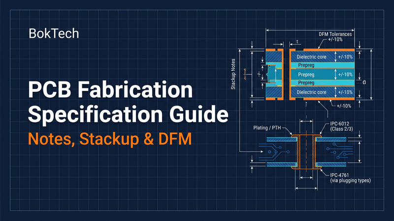
Quick Takeaway (TL;DR): A PCB fabrication specification (Master Fabrication Drawing) is the legally binding engineering contract that translates CAD vector geometry into a physical, buildable circuit board. While Gerber or ODB++ files describe two-dimensional X/Y copper shapes, they convey zero data regarding Z-axis stack-up construction, raw laminate dielectric properties (Dk/Df), finished plating tolerances, hole wall copper thickness (20 µm vs. 25 µm), or IPC acceptance thresholds. Leaving these variables undefined forces fabricators to guess your intent, adding 15% to 30% risk padding to quotes or triggering engineering holds. An actionable specification establishes explicit mechanical tolerances (±10% board thickness), material callouts (specific Tg and laminate families), IPC-4761 via protection types, and IPC-6012 Class 2 vs. Class 3 inspection criteria before CAM tooling begins.
1. The Anatomy of a Manufacturing Specification: Geometry vs. Process
A complete PCB production data release consists of two complementary halves: the geometric dataset (Gerber RS-274X, Gerber X2, or ODB++) and the fabrication specification (embedded in the master drawing notes or a formal fabrication document).
Relying on Gerber data alone guarantees manufacturing ambiguity. The table below delineates the clear division of responsibility between vector artwork and specification notes:
| Engineering Dimension | What Gerber / ODB++ Files Convey | What the PCB Fabrication Specification Must Define |
| Layer Ordering & Z-Axis | 2D layout of individual copper layers | Physical layer sequence, dielectric core/prepreg thicknesses, and total board thickness |
| Dielectric Substrate | None (Files represent pure spatial voids) | Base material family (e.g., IT-180A, Megtron 6), glass transition temperature (Tg), and Dk/Df |
| Copper Foil & Plating | Feature boundaries and trace tracks | Starting base copper weight (0.5 oz, 1.0 oz) and minimum finished plated copper thickness |
| Hole Processing | X/Y drill coordinates and tool diameters | Finished hole size (FHS) tolerances, PTH vs. NPTH designation, and press-fit requirements |
| Via Treatment | Pad openings and hole placements | IPC-4761 via type (tented, resin plugged, copper-capped VIPPO) |
| Signal Integrity | Nominal drawn trace widths and spacings | Target single-ended/differential impedance values, layer reference planes, and ±7% to ±10% tolerance |
| Quality & Inspection | None | IPC-6012 Class 2 or Class 3 acceptance, coupon micro-sectioning, and netlist testing criteria |
2. Mechanical and Structural Dimensional Fields
The mechanical envelope sets the tooling boundaries, CNC routing programs, and panel utilization limits before any electrical processing begins.
Finished Board Thickness and Stack-Up Tolerances
Nominal board thickness (commonly 1.6mm / 0.062 in) is the cumulative sum of laminated copper foils, dielectric cores, prepreg bonding plies, and outer soldermask layers.
•Standard Thickness Tolerance: ±10% of nominal thickness (e.g., 1.60mm ± 0.16mm).
•Tight Mechanical Tolerance: ±8% or ±0.10mm, required for edge-card connections (PCIe add-in cards) to ensure reliable contact mating inside enclosure card guides.
•Critical Mating Zones: If a specific region (such as a gold finger contact edge) requires a tighter tolerance than the general board body, call out that zone independently on the mechanical drawing.
CNC Routing, V-Scoring, and Outline Tolerances
Provide the finished board outline on a dedicated mechanical CAD layer with fully closed vector geometry.
•CNC Routing Tolerance: Standard profile routing holds ±0.13mm (±0.005 in); high-precision routing holds ±0.08mm (±0.003 in).
•V-Scoring Specifications: Define the score angle (typically 30° or 45°) and the remaining web thickness (usually 1/3 of board thickness ±0.10mm).
•Breakaway Tabs and Mouse-Bites: If panelized with perforated breakaway tabs, specify whether tab protrusion is permitted past the board edge after de-paneling or if flush breakout is mandatory.
Drill Hole Tolerances and Aspect Ratio
Drill files convey XY hit locations, but master drawing notes must explicitly define post-plating finished hole sizes (FHS):
Finished Aspect Ratio Formula: Aspect Ratio = Total Board Thickness ÷ Smallest Plated Drill Hole Diameter
•Plated Through-Hole (PTH) Tolerance: Typically ±0.05mm (±0.002 in) to ±0.08mm.
•Non-Plated Through-Hole (NPTH) Tolerance: Typically ±0.05mm (±0.002 in).
•Press-Fit Compliance: Compliant pin holes require a strict finished tolerance of ±0.025mm (±0.001 in) to ensure reliable gas-tight mechanical retention without damaging connector pins.
•Aspect Ratio Limits: Standard through-hole plating reliably handles aspect ratios up to 8:1 to 10:1. Pushing aspect ratios to 12:1 or higher requires specialized continuous chemical agitation and continuous-current electroplating to prevent thin copper plating in the center of the via barrel.
| Mechanical Feature | Standard Commercial Tolerance | Precision / High-Reliability Tolerance | Manufacturing Impact If Uncontrolled |
| Finished Thickness | ± 10% of nominal | ± 8% (or ± 0.10mm for PCIe edge fingers) | Edge-card connector insertion failure or loose contact |
| Board Outline (CNC) | ± 0.13mm (± 0.005 in) | ± 0.08mm (± 0.003 in) | Interference fits inside tight aluminum enclosures |
| PTH Finished Diameter | ± 0.08mm (± 0.003 in) | ± 0.05mm (± 0.002 in) | Solder bridging or poor barrel fill on pin headers |
| NPTH Finished Diameter | ± 0.05mm (± 0.002 in) | ± 0.025mm (± 0.001 in) | Loose tooling alignment pins or mechanical standoff play |
| Internal Annular Ring | Breakout permitted up to 90° | ≥ 2.0 mil (50 µm) minimum (IPC Class 3) | Via barrel cracking under high thermal cycling stress |
Review our comprehensive PCB manufacturing services for standard tooling capabilities, and explore dedicated guidelines for HDI and microvia builds.
3. Dielectric Materials and Electrical Parameters
Material and electrical definitions determine high-speed signal integrity, thermal dissipation, and long-term operating life.
Base Laminate System Callouts
Never state simply "FR-4" on an engineering drawing. Standard FR-4 covers an enormous span of chemical formulations, glass weave styles, and thermal endurance ratings.
•Standard Baseline: High-Tg FR-4 (e.g., ITEQ IT-180A, Shengyi S1000-2M) featuring Tg ≥ 170°C, Td ≥ 340°C, and low Z-axis thermal expansion (CTE ≤ 45 ppm/°C).
•Ultra-Low-Loss Computing: For 56G/112G PAM4 and PCIe Gen 5/6, call out exact brand families such as Panasonic Megtron 6 (Df ≈ 0.002) or Megtron 7 (Df ≈ 0.001).
•High-Frequency RF / PTFE: Call out Rogers RO4350B, RO4003C, or Taconic materials, specifying required dielectric constant (Dk) tolerances at specific test frequencies (e.g., Dk = 3.48 ± 0.05 @ 10 GHz).
Copper Weight Specification
Always differentiate between base copper foil weight and finished plated copper weight:
•Outer Layers: A drawing specifying "1.0 oz finished copper" typically begins with 0.5 oz (18 µm) base foil, electroplating an additional 0.5 oz of copper in the through-hole barrels and surface tracks to reach ~35 µm final thickness.
•Inner Layers: Inner layers do not receive electroplating; a "2.0 oz inner layer" must be constructed from full-weight 70 µm foil cores.
•Heavy Copper (3 oz to 5 oz): Heavy copper planes require specialized etch compensation factors. State minimum track width and spacing constraints in accordance with the heavier copper foil.
Controlled Impedance Callouts
An impedance specification is only actionable if it links electrical targets to physical geometries and reference layers. Provide an impedance table formatted directly on the master drawing:
| Layer Number | Trace Type / Configuration | Target Impedance | Manufacturing Tolerance | Reference Planes | Nominal Trace / Space (W/S) |
| Layer 1 (Outer) | Single-Ended Microstrip | 50.0 Ω | ± 10% (± 5.0 Ω) | Layer 2 (Ground) | 4.5 mil / N/A |
| Layer 1 (Outer) | Differential Pair Microstrip | 90.0 Ω (USB 2.0/3.0) | ± 10% (± 9.0 Ω) | Layer 2 (Ground) | 4.0 mil / 5.0 mil space |
| Layer 3 (Inner) | Differential Stripline (PCIe Gen 5) | 85.0 Ω Differential | ± 7% (± 5.9 Ω) | Layer 2 & Layer 4 (Ground) | 4.2 mil / 6.0 mil space |
| Layer 3 (Inner) | High-Speed SERDES (112G PAM4) | 100.0 Ω Differential | ± 7% (± 7.0 Ω) | Layer 2 & Layer 4 (Ground) | 3.8 mil / 7.2 mil space |
4. Fabrication Notes & IPC Class 2 vs. Class 3 Acceptance Criteria
Standard fabrication notes communicate process rules, chemical plating types, and post-processing treatments.
Surface Finish Selection
Specify the exact surface finish standard and plating thickness ranges:
•Lead-Free HASL: Standard low-cost finish; acceptable for basic passives and through-hole parts, but unsuitable for fine-pitch BGAs (< 0.8mm) due to uneven surface doming.
•Electroless Nickel Immersion Gold (ENIG): IPC-4552 standard; requires 120–200 µin (3–5 µm) nickel under 2–3 µin (0.05–0.075 µm) immersion gold. Guarantees flat pad coplanarity for BGA and 0201/01005 assembly.
•ENEPIG: IPC-4556 standard; adds an intermediate 2–12 µin (0.05–0.30 µm) palladium barrier layer to eliminate "black pad" corrosion risks, ideal for high-reliability wire-bonding and multi-pass lead-free reflow.
IPC-4761 Via Protection Definitions
Clearly define how vias must be treated during fabrication to prevent solder wicking and outgassing:
•Type II (Tented & Covered): Soldermask covers the via annular ring and barrel opening from one or both sides (standard low-cost processing).
•Type III / IV (Plugged): Via barrel is plugged with non-conductive epoxy paste or soldermask ink, preventing solder ingress.
•Type VII (Filled and Capped - VIPPO): Via barrel is completely plugged with non-conductive resin, cured, planarized flush with the copper foil, and electroplated with copper. Mandatory for Via-in-Pad locations under 0.4mm–0.5mm BGA footprints.
IPC-6012 Class 2 vs. Class 3 Acceptance Standards
Clearly state whether the finished board must be inspected against IPC-6012 Class 2 (Dedicated Service Electronic Products) or IPC-6012 Class 3 (High-Reliability Electronic Products):
| Inspection Parameter | IPC-6012 Class 2 (Commercial / Industrial) | IPC-6012 Class 3 (Mission-Critical / Aerospace) | Failure Mode Prevented by Class 3 |
| Through-Hole Copper Plating | Average 20 µm (0.8 mil); Min thin spot 18 µm | Average 25 µm (1.0 mil); Min thin spot 20 µm | Via barrel fatigue cracking under repeated thermal cycles |
| Internal Annular Ring | Minimum 1.0 mil (25 µm); 90° breakout allowed | Minimum 2.0 mil (50 µm); Zero breakout permitted | Internal trace-to-via connection separation under thermal shock |
| Dielectric Spacing | Minimum 3.5 mil (89 µm) post-lamination | Minimum 3.5 mil (or as engineered for high voltage) | High-voltage breakdown and inner-layer dendrite growth |
| Conductor Imperfections | Up to 20% width reduction permitted | Maximum 10% to 15% width reduction permitted | Localized conductor necking, hot spots, and impedance drift |
| Coupon Verification | Optional / Batch sample inspection | Mandatory micro-section coupons per production panel | Latent plating voids escaping to field assembly |
For stack-up layer parameters and manufacturing allowances, consult PCB fabrication specifications: layer stack, thickness and tolerances.
5. Master Drawing Checklist: Fields Required for First-Pass DFM Sign-Off
To ensure your data package moves directly into production without delays, compile your master drawing using this checklist:
| Specification Domain | Required Parameters to Document | Engineering Purpose | Quoting & Production Risk If Omitted |
| 1. Header & Revisions | Part number, board title, current revision, date | Establishes configuration control | Fabricator builds against obsolete drawing revision |
| 2. Construction Type | Multilayer, HDI (1+N+1 to 3+N+3), Rigid-Flex, IMS | Identifies sequential press cycles | Incorrect tooling cost and misquoted production lead times |
| 3. Material Callout | Base laminate brand/family, Tg, Td, CTI, Dk/Df | Dictates thermal and high-speed behavior | Low-Tg material substituted, causing delamination during reflow |
| 4. Copper Specifications | Base copper foil + finished plated copper per layer | Controls current capacity and minimum trace etch | Under-etched fine traces or insufficient PDN current capacity |
| 5. Soldermask & Legend | LPI Soldermask color/brand, finish (glossy/matte), silkscreen color | Protects copper and guides debugging | Mask bridging breakdown between fine-pitch SMT pads |
| 6. Via Processing | IPC-4761 Type designation per hole class; VIPPO callout | Controls via filling and surface planarity | Solder wicking into open vias under BGA footprints |
| 7. Impedance Matrix | Target Ohms, tolerance, trace width/space, reference layers | Guarantees signal integrity across channels | Severe reflections and link budget failure on SERDES |
| 8. Testing & Quality | 100% Netlist test, IPC Class 2/3, microsection coupons | Establishes quality acceptance rules | Disputed scrap liability on border-line annular ring defects |
6. Separating Bare-Board Fab Notes from PCBA Assembly Specifications
A common procurement mistake is combining bare-board fabrication instructions with surface-mount assembly instructions into a single confusing document.
Bare-board fabricators must never be forced to extract manufacturing data from assembly drawings, and SMT assembly engineers should not have to parse raw laminate press profiles. Keep these two disciplines separated into dedicated documents:
| Specification Scope | Bare-Board Fabrication Drawing (Fab Notes) | PCBA Assembly Drawing (SMT / THT Notes) |
| Primary Audience | PCB manufacturing plant CAM & process engineers | SMT machine operators, quality inspectors, process engineers |
| Key Input Files | Gerber / ODB++, Excellon drill, Stack-up drawing | Bill of Materials (BOM), Centroid (Pick-and-Place), Schematic |
| Core Content | Dielectric materials, copper weights, hole plating, finishes | Component part numbers, polarities, pin-1 markers, DNP parts |
| Process Instructions | Lamination press cycle, back-drilling, gold finger beveling | Reflow profile guidelines, selective soldering, underfill notes |
| Acceptance Standard | IPC-6012 (Bare board quality and structural integrity) | IPC-A-610 (Acceptability of electronic assemblies) |
Review our PCB assembly services: prototype to low-volume to understand how bare boards transition smoothly into automated assembly.
7. Frequently Asked Questions (FAQ)
Why can't a PCB fabricator infer the layer stack-up directly from Gerber files?
Gerber files only represent 2D vector shapes. They contain no physical data regarding the order of internal copper layers, the required dielectric core thicknesses, the prepreg resin content, or the target finished board thickness. An explicit stack-up drawing is mandatory to define layer sequence and dielectric spacing.
What is the difference between tool size and finished hole size in drill notes?
Tool size (drill bit diameter) is the physical size of the CNC drill. Finished hole size (FHS) is the final internal diameter of the hole after chemical desmear, electroless copper seed deposition, and electrolytic barrel plating (which typically adds 25 µm to 35 µm of copper to the hole walls). Fabrication notes should always state the required finished hole size (FHS) so the CAM engineer can apply the proper drill over-sizing compensation.
How do I specify controlled impedance if I do not know the fabricator's exact prepreg inventory?
Specify the target electrical impedance, the tolerance (typically ±10%), the trace width and spacing, and the designated reference planes. Include a note stating: "Trace width and dielectric thickness may be adjusted by the fabricator to meet target impedance, subject to engineering approval prior to tooling."
What happens if I specify IPC Class 3 without updating CAD design rules?
If your CAD layout was designed using standard Class 2 annular rings (1.0 mil internal ring) and you mandate IPC-6012 Class 3 on the drawing (requiring minimum 2.0 mil internal ring), the manufacturing panel will fail micro-section inspection due to annular ring breakout. Design rules in CAD must be aligned with IPC Class 3 requirements before routing begins.
8. From Prototype to Full-Scale Production: Partner with BokTech
Translating an advanced hardware design into a defect-free production run requires seamless collaboration between design engineering and factory manufacturing capabilities:
•Holding tight ±8% board thickness tolerances across 10 to 32 layer high-density stack-ups.
•Achieving 100% IPC-4761 Type VII VIPPO planarization on 0.35mm–0.50mm micro-BGAs without solder voiding.
•Maintaining controlled impedance tolerances within ±7% on 112G PAM4, PCIe Gen 5/6, and DDR5 buses.
•Processing exotic high-frequency materials (Panasonic Megtron 6/7, Rogers 4000 series, ITEQ high-Tg FR-4) in certified hybrid stack-ups.
BokTech delivers end-to-end turnkey PCB manufacturing, high-precision SMT assembly, and complete box-build integration from our advanced facility in Shenzhen. We provide:
•Precision Multi-Layer Fabrication: 1 to 32 layer capability supporting Any-Layer HDI, heavy copper power planes (up to 5 oz), and automated controlled-depth back-drilling with residual stubs verified under 6 mils.
•IPC-6012 Class 3 Certification: Complete micro-section coupon reporting, thermal stress testing, and 100% electrical netlist testing on flying probe and dedicated fixture testers.
•Advanced In-House SMT Assembly: Automated pick-and-place lines handling 01005 passives, 0.35mm micro-BGAs, Package-on-Package (PoP), and selective wave soldering under IPC-A-610 Class 2 and Class 3 standards.
•Rigorous Quality Verification: 100% 3D Solder Paste Inspection (SPI), high-resolution 3D Automated X-Ray (AXI), Automated Optical Inspection (AOI), and functional test fixture development.
•Comprehensive Pre-Production DFM Reviews: Every design package undergoes a thorough engineering audit to verify stack-up symmetry, validate aspect ratios, and eliminate specification ambiguities before CAM tooling begins.
To prepare your dataset for fabrication sign-off, review our PCB requirements for manufacturing files, inspect our frequently asked questions, and explore our quick-turn PCB prototype service to begin testing your concepts.
Ready to manufacture your multi-layer PCB or custom PCBA? Upload your PCB files for an instant quotation, or contact our engineering team today for a complete DFM and stack-up review.


{{ commentCount }} Comments