SMT Stencil
- By : Project team
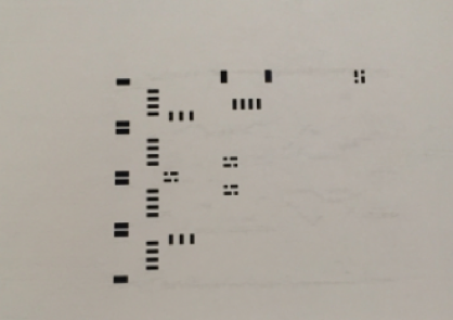
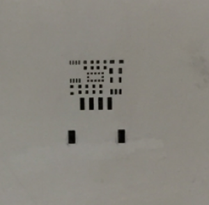
The sole purpose of an SMT stencil is to transfer solder paste to a bare circuit board. A stainless steel foil is laser cut creating an opening for every surface mount device on the board. Once the stencil is properly aligned on top of the board, solder paste is applied over the openings (making a single pass, using a metal squeegee blade). When the stainless steel foil is separated from the board, solder paste will remain, ready for placement of the SMD. This process, as opposed to hand soldering methods, ensures consistency and saves time.
Stainless steel stencil thickness and aperture opening size control the volume of paste deposited on the board. Too much solder paste causes solder balling, bridging, and tomb-stoning. A lack of solder paste creates insufficient solder joints. All of which compromise the electrical functionality of the board.
Proper Stencil thickness is chosen based on the types of devices being loaded on the board. For most components like 0402 Packaging resistors/capacitors or 0.8mm pitch Chips, recommend to use 0.1/0.12mm thickness stencil works. For these boards with BGA or other 0.5 pitch chips, recommend to use 0.08mm electro-polishing stencil.
The following types are available on BokTech.


Note:
1. Electro-polishing is special process to remove these micro remains on the stencil after laser cutting which is very helpful to print the solder paste on the pads smoothly, especially for these small pitch chips’ pads.
2. Stencil is usually laser cutting according to the ‘Projectname.GTP/GBP’ layer in gerber. For these PCB without small pitch chips, stencil can also be laser cutting according to Projectname.GTS/GBS & Projectname.TXT & Projectname.GTO/GBO, but not recommended.
- Prev : Test Process
- Next : Quality Control Process

