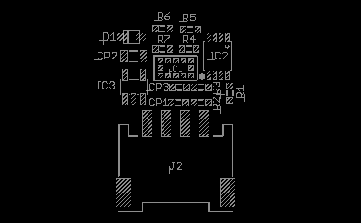
Components Layout
- By : Project team
"Components Layout" is a reference file for assemble the components to PCB.
In this file, you need to add the reference part of all components. You also need to mark the first pin of Chips and the positive pole of diodes to avoid unnecessary mistakes.
This file is extremely helpful for doing QA & QC.
Note:
1. For Resistor, we usually mark as R1, R2…
2. For capacitor, we usually mark as C1, C3…
3. For Diodes, we usually mark as D1, D2…
4. For Chips, we usually mark as IC1, IC2…
5. For connectors, we usually mark as J1, J2…

- Prev : PCB specification
- Next : Test Process

