
Gerber File Format Complete Guide: Layers, RS-274X & Submission Rules
- By : Project team
Gerber File Format Complete Guide: Layers, RS-274X & Submission Rules
Summary: The Gerber format is the de facto standard for describing printed circuit board (PCB) images in the electronics manufacturing industry. This guide explains what Gerber files are, the complete layer stack required for fabrication, the RS-274X and Excellon drill specifications, and the five submission rules that help engineers pass PCB prototyping review on the first try.
In the PCB design-to-manufacturing workflow, the Gerber file plays the role of the "production blueprint." No matter which EDA (Electronic Design Automation) or CAD tool you use—Altium Designer, KiCad, Eagle, OrCAD, or others—you must export your finished layout to the Gerber format before a bare-board fabricator can build it.
This article is written for hardware engineers, PCB buyers, and makers. It gives you a clear layer checklist + format spec + submission checklist so you can prepare fabrication-ready files with confidence.
Table of Contents
1. What Is a Gerber File?
Gerber is an open ASCII vector format for 2D binary images. It is the de facto standard used by printed circuit board (PCB) industry software to describe PCB images and is the core data exchanged in PCB fabrication.
In plain terms: your EDA tool draws the design; Gerber exports the machine-readable production instructions. The fabricator's CAM (Computer-Aided Manufacturing) system reads the Gerber data and prepares outputs for every production step—exposure, etching, drilling, solder masking, silkscreen, and testing.
2. Why Gerber Matters in PCB Fabrication
A typical PCB fabrication data flow looks like this:
1. The design is completed in an EDA / CAD system (schematic + PCB layout).
2. One Gerber file is exported per image layer (copper layers, solder mask, legend/silkscreen, board outline, etc.).
3. Drilled hole information is usually provided separately as an Excellon-format drill file (for historic reasons; Gerber can also express drills).
4. All files are zipped into a single archive and sent to the PCB bare-board shop.
5. The fabricator loads the archive into a CAM system to generate film, drill tapes, and test data, then moves into real production.
Bottom line: No valid Gerber, no valid PCB.
3. Which Gerber Layers Does a Complete PCB Contain?
The table below uses a common 4-layer board as the example and lists the standard file extensions (case-insensitive; the naming below is the most widely recognized convention):
| Extension | Layer Name | Description | Required? |
|---|---|---|---|
Projectname.GTL | Top Layer | Top copper / trace layer | ✅ Yes |
Projectname.GL2 | Inner Layer 2 | Inner layer 2 (4-layer board) | ✅ Yes (4L+) |
Projectname.GL3 | Inner Layer 3 | Inner layer 3 (4-layer board) | ✅ Yes (4L+) |
Projectname.GBL | Bottom Layer | Bottom copper / trace layer | ✅ Yes |
Projectname.GTS | Top Solder Mask | Top solder mask (green mask openings) | ✅ Yes |
Projectname.GBS | Bottom Solder Mask | Bottom solder mask | ✅ Yes |
Projectname.GTO | Top Silk / Legend | Top silkscreen (text, logos) | ✅ Recommended |
Projectname.GBO | Bottom Silk / Legend | Bottom silkscreen | ⚪ Optional |
Projectname.GKO / GML | Board Outline | Board outline / milling profile | ✅ Yes |
Projectname.TXT | Drill Drawing | Drill file (Excellon format) | ✅ Yes |
Projectname.GTP | Top Solder Paste | Top stencil paste layer | ⚪ Not for PCB (needed for stencil) |
Projectname.GBP | Bottom Solder Paste | Bottom stencil paste layer | ⚪ Not for PCB (needed for stencil) |
Note: A 2-layer board (the most common) typically includes only GTL, GBL, GTS, GBS, GTO, (GBO), GKO, and TXT. Inner layers GL2 / GL3 exist only on 4-layer and thicker stacks.
4. Layer-by-Layer Explanation
• GTL / GBL (Top / Bottom Copper): Carry the traces and pads—the "circuit body" of the PCB.
• GL2 / GL3 (Inner Layers): Power, ground, or signal layers inside multilayer boards, laminated with prepreg.
• GTS / GBS (Solder Mask): Define where solder mask (green oil) is opened—i.e., where pads are exposed and where they are covered. Note the solder mask is negative logic: where the Gerber has graphics, the mask is actually removed.
• GTO / GBO (Silkscreen): Text, logos, and polarity marks printed on the board surface for assembly and inspection.
• GKO / GML (Board Outline): Defines the PCB outer profile and slots—the basis for CNC routing.
• TXT (Drill File): Records coordinates, hole sizes, and attributes of all vias and component holes in Excellon format.
• GTP / GBP (Paste Layers): Stencil apertures for SMT. Not required for PCB production, but mandatory if you later make a solder stencil.
5. Gerber & Drill File Format Requirements
1. Gerber must be RS-274X format (also called Extended Gerber). RS-274X embeds aperture definitions, units, and polarity inside the file—no separate aperture list needed—and is the current industry standard.
2. The drill file (
Projectname.TXT) should be Excellon format. Excellon is the widely compatible coordinate + hole-size description read by drilling machines.3. Different EDA tools export slightly different extensions (e.g., variants beyond
.GTP), but the content is equivalent and all are accepted; the extensions listed here are the most common and easiest for fabricators' Gerber viewers to recognize.
Tip: When exporting, choose "RS-274X (Extended)" and confirm that units (metric mm / imperial mil), decimal precision, and zero suppression match your fabricator's requirements.
6. Five Critical Submission Rules for PCB Houses
To avoid prototyping failures caused by missing or misplaced files, follow these rules:
1. Use RS-274X for all Gerber files. Legacy RS-274D requires a separate aperture list and is error-prone—not recommended.
2. The drill file (
Projectname.TXT) must be Excellon format and match the Gerber set.3. Keep Gerber files and the drill file in the same folder (same ZIP root). Storing them separately makes it easy for CAM engineers to overlook the drill data, causing "missing holes" or layer mismatch.
4. GTP / GBP (paste layers) are not required for PCB production, but submit them if you will later make an SMT stencil, to avoid a second file round-trip.
5. Different software extensions are all acceptable; the extensions in this article are the most universal and recognizable by Gerber viewers—prefer them when possible.
✅ Pre-submission checklist: Top/bottom copper present → solder mask present → board outline present → drill file (Excellon) in the same archive → units & polarity confirmed → ZIP and send.
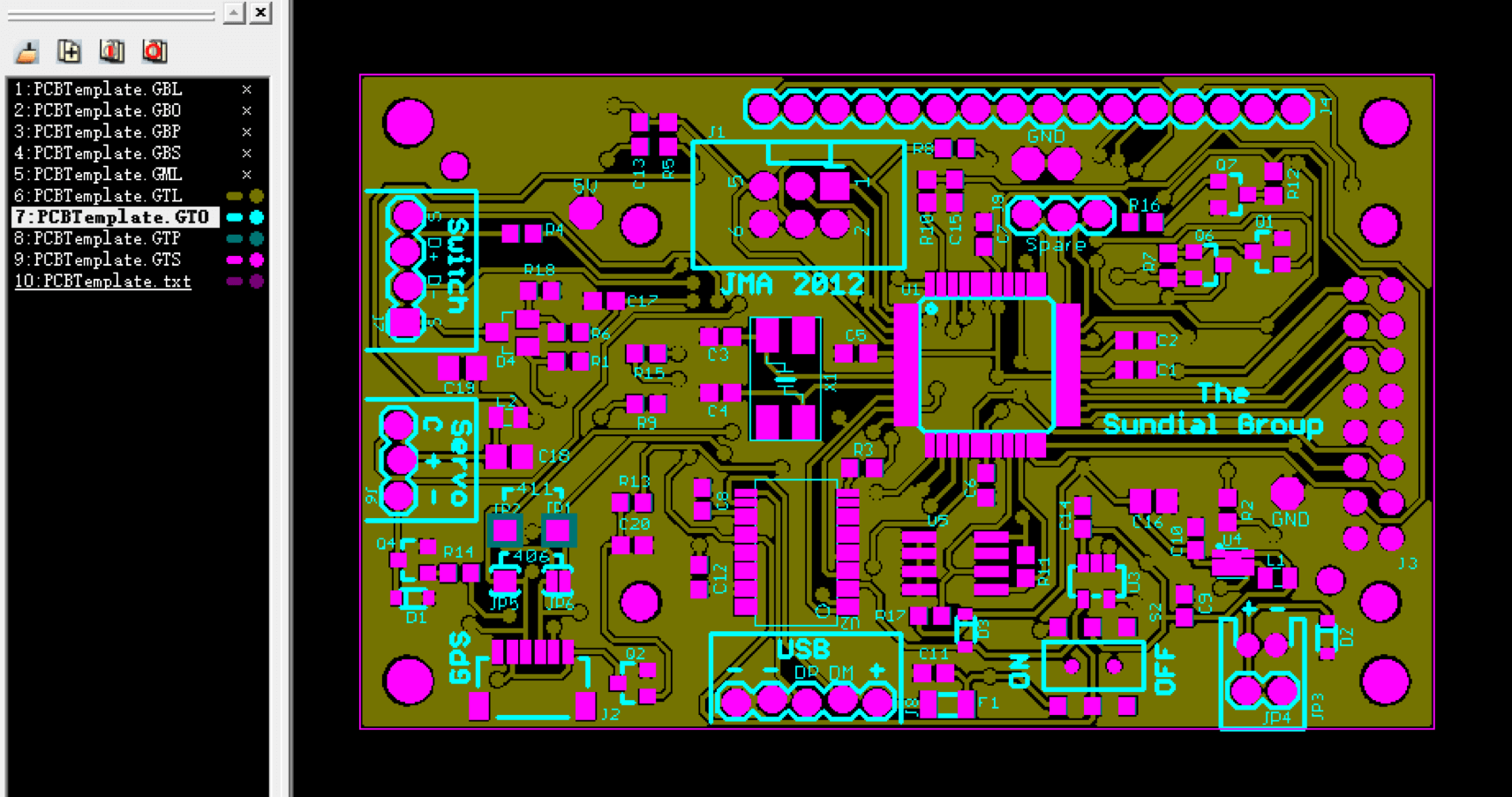
7. Gerber Template Preview
Below is a standard Gerber layer template you can use to verify your project is complete:Tip: A downloadable Gerber template is available on the right (original article)—apply the naming convention directly to reduce communication overhead.
Rename your image togerber-template.pngand place it in theimages/directory before publishing.
8. Frequently Asked Questions
Q1: What is the difference between Gerber and the PCB source file (e.g., .PcbDoc)?
A: The source file is the editable EDA project and cannot be produced directly. Gerber is the exported photoplot data. For prototyping you only need Gerber (plus drill), not the source.
Q2: How many Gerber layers differ between 2-layer and 4-layer boards?
A: A 2-layer board is typically 7–8 files (excluding bottom silkscreen and paste); a 4-layer board adds GL2 and GL3 inner layers, totaling about 9–10 files.
Q3: The solder mask is negative—what should I watch for when exporting?
A: Confirm the solder mask polarity is set to Negative in your EDA export, and that the opening size matches your pads, or you may end up with "pads that should be exposed are covered."
Q4: Can the drill file be replaced by Gerber?
A: Yes, but Excellon remains the industry convention. As long as the fabricator's CAM supports it and you label it clearly, Gerber-expressed drills are also acceptable.
Q5: Will different file extensions affect production?
A: They do not affect recognition as long as the format is correct. Using common extensions (GTL/GBL/GTS…) significantly lowers miscommunication and misjudgment risk.
9. Conclusion & Call to Action
Preparing Gerber files is only the first step to successful PCB prototyping. With the layer checklist + RS-274X / Excellon spec + same-archive submission method in this guide, you can essentially achieve "submit once, pass once."
• 📥 Need a standard Gerber template? Download the template on the right and apply the naming convention directly.
• 🚀 Ready to prototype or mass-produce? Send your ZIP archive to the Boktech PCB service page for a fast quote and technical review.
• 💡 Not sure your files are valid? Our CAM engineering team offers free pre-check to catch open circuits, shorts, and drill misalignment before production.
Compiled by the Boktech technical team. Please credit the source when reposting. For more PCB fabrication insights, follow www.boktech.cc.
Related reading (internal link placeholders—replace with real on-site URLs): PCB Prototyping Workflow / Impedance Control Design / Multilayer Stack-up Structure / SMT Stencil Making Guide
- Prev : No More
- Next : BOM (bill of materials)
